Modchips of the State
This is the annotated transcript for my 35C3 talk, "Modchips of the State" about the technical feasibility of the BMC implant described in the Bloomberg article from October 2018. You can also watch the 40 minute video if you prefer. Both the video, presentation slides and images are CC-BY licensed.
Disclaimers
 Before we begin, I need to add a disclaimer that I don't know the story behind the story: none of us outside of Bloomberg know their sources and we don't know the truth of their sources' allegations. This talk is based on my experience over the past several years, both on the offensive side with firmware proof of concept attacks like Thunderstrike and Thunderstrike 2 against Apple's Macbooks, as well as my work on the defensive side with the Heads firmware for slightly more secure laptops and the LinuxBoot open firmware for servers. So while I don't know the exact details, I have been thinking quite a bit about how to build and defend against hardware implants.
Overview
 That's why I was very excited when Jordan Robertson and Michael Riley's Bloomberg article was released. One of the parts that really intrigued me is that the photo illustration by Scott Gellber, which is an "artists conception" not a photo of an actual implant, positioned the alleged device exactly where I would have installed it: on an unused 8 pin SOIC footprint between the BMC flash and the BMC CPU. This indicated to me that the article had received sufficient technical review, which is a rarity in tech reporting.
 The immediate responses from the security community varied from agreement that it was reasonable to that supply chains were dangerously unprotected to that it was implausible, many groups pulled their machines apart, and in general ended up with no consensus.
The Big Hack
 Let's have a quick review of some of the claims alleged in the "Big Hack" article.
according to one person familiar with the process ... the testers found a tiny microchip, not much bigger than a grain of rice, that wasn’t part of the boards’ original design. Amazon reported the discovery to U.S. authorities
they looked more like signal conditioning couplers, another common motherboard component, than microchips,
The illicit chips were connected to the baseboard management controller ... giving them access to the most sensitive code even on machines that have crashed or are turned off.
 This last claim sounds sort of extreme, but that is exactly the role of the baseboard management controller, or BMC. It running anytime the server has AC power and is connected to the power supply so that it can turn the x86 CPU on and off. Since most sites want to do this remotely, it also has network access either through its own NIC or through sharing the LAN-on-motherboard (LOM) NIC. Many sites also want a remote serial console, so it intercepts the serial ports from the x86. It can also provide fake USB mass-storage devices for automated OS installation. Lots of sites want remote KVM, so the BMC can also provide a VGA interface, which means that it is on the PCIe bus and can DMA against x86 memory. Additionally on many systems it is muxed into the SPI bus for remote firmware updates as well as into the LPC bus, giving it access to the TPM. This is a really dangerous place to have malware, especially since as Yigal Edery, the program manager for Azure security, pointed out at OCP EU'18, it is "typically unsecure with no protection, no detection and no recovery".
Additionally, Bloomberg alleges that:
One official says investigators found that it eventually affected almost 30 companies, including a major bank, government contractors, and Apple Inc
Three senior insiders at Apple say that in the summer of 2015, it found malicious chips on Supermicro motherboards ... and reported the incident to the FBI.
Apple severed ties with Supermicro the following year, for what it described as unrelated reasons.
This last one was quite interesting since it potentially corroborates the 2017 story about Apple "axing Supermicro servers from their data centers". There had been no followups on this story other than Apple denying it, so it was intriguing to see it come up again.
These last two claims were more worrysome:
In one case the malicious chips were thin enough that they'd been embedded between the layers of the PCB, according to one person who saw pictures of the chips.
The chips had been inserted during the manufacturing process, two officials say, by operatives from a unit of China's People's Liberation Army'
The Big Denials
The story had all anonymous sources, although Bloomberg stands by their sources, including "six current and former senior national security officials", "two people inside AWS" and "three senior insiders at Apple". They go on to claim that "in all, 17 people confirmed the manipulation of Supermicro's hardware and other elements of the attacks". Which seems like strong support, except that everyone allegedly involved publicly denies it,
 The Director of National Intelligence gave a speech claiming to "have seen no evidence of the supply chain hack detailed in the Bloomberg story**". Another NSA official worried that the security community was "_chasing shadows".
 |
 |
Amazon's CISO, Steve Schmidt, wrote their denial, saying that:
at no time have we ever found any issues relating to modified hardware or malicious chips in Supermicro motherboards, nor have we engaged in an investigation with the government
Apple's CEO, Tim Cook, was even more blunt: "**There is no truth to this. This did not happen."
 Supermicro's CEO, Charles Liang, wrote a letter to customers, in which he also denied the story and discussed the steps that they are taking to secure their supply chain. Let's examine some of the things they're doing to protect the manufacturing process.
Supply Chain
PCB Manufacturing
Supermicro's CEO writes in the "Supply Chain Management" section:
Our manufacturing process is designed to prevent unauthorized physical alterations of our motherboards by either our contract manufacturers or anyone at Supermicro.
If any single contractor attempts to modify the designs, the manufacturing process is structured so that those alterations would not match the other design elements in the manufacturing process.

On a recent holiday in China, I visited a PCB manufacturing company in Guangzhou to see what is involved in producing PCBs and what would be required to subvert the process. These are not photos from Supermicro's factories, they are just illustrative of the steps.
If the hardware implant requires any additional through-holes or blind vias, they would need to modify the drill files prior to the bare boards going to the drill rack and electroplating step. Any additional traces would require subverting the masking/etching step to add the additional traces to the copper layer. Changes in either of these steps would be detected at the automated optical inspection stage, where the bare PCB layer is scanned and compared to the desired file.
 For an implant to be installed between the PCB layers, it would need to be installed during the lamination stage. Unless the design calls for embedded passives, this stage typically does not involve any soldering or component installation, so those tools would be out of place in the workroom. Additionally, any components installed during that lamination would have to not change any of the electrical conductivity since the flying probe testers or "bed of nails" will detect the change. Since the bed-of-nails test is a physical artifact, either it or the test software would require modification to ignore any changes.
The other problem with making changes at these stages is that it is very difficult to contain it to a single target. The factories that make mainboards are producing an enormous number of them and, unless they are very custom designs, do not have any idea where the boards will end up. Any implants risk being shipped to customers who might discover them, and if the parts are inside the PCB there is no good cover story for how they ended up there.
PCB Assembly
Supermicro's CEO also wrote that:
Our employees are on site with our assembly contractors throughout the process.
 |
 |
In my discussions with companies doing contract manufacturing in China, they also said that it was necessary to have their representatives in the factory during PCB assembly. They discussed the difficulty in finding trusted representatives and many of them had relocated employees to Shenzhen to supervise production runs. Even then some of them had trouble finding trusted representatives, as Keyboard.io found out. (Again, these photos are of my trip to a PCBA factory in Shenzhen, not Supermicro's)
 The main concern that most companies have is that their new components will be substituted for lower-cost, salvaged parts. In the markets of Huaqiangbei you can see people desoldering parts from e-waste, sorting the parts into bins and selling the salvaged components by the kilo for fractions of the original prices. One company told me that there was a 100% chance that the pick-and-place reels would be loaded with cheap parts if they didn't have someone onsite to supervise.
 Salvaged parts might be a reliability concern, but more concerning from a security perspective are counterfeit parts like these fake FTDI serial chips analyzed by Zeptobars. They are marked identically, but inside have completely different implementations and could be carrying arbitrary backdoor functionality. For this reason, some companies told me that they send their representatives to the PCBA with reels of high value components purchased from trusted supplies to be mounted on the PNP machine and then watch to be sure that their parts are placed on the boards.
Spot-checks
Supermicro's CEO also writes:
We also periodically employ spot checks and x-ray scans of our motherboards.
Our test processes at every step are not only designed to check functionality, but also to check for the integrity and composition of our designs and to alert us to any discrepancies in the base design.

X-Ray inspection would detect any implants between layers as well as any active components that are masquerading as passives. The active 8-SOIC chips is clearly different from the passive resistor and capacitor, although it would not necessarily detect the difference between the two FTDI chips shown above.
Also of interest in that X-Ray is the inductor in the DIP package. Many Ethernet components involve transformers, so they often contain these sorts of components. Some people have reported finding odd hardware in their Ethernet jacks and jumped to the conclusion that they must be some sort of implant, but they were more likely this sort of integrated magnetics.
 Sophia D'Antoine with River Loop Security was commissioned to pull apart a Supermicro board. She found places were the silkscreen on the mainboard didn't match the components installed and at least one component installed on a test pad, but after x-ray analysis determined it to be a passive inductor instead of an implant. There are also many places were Supermicro puts extra pads on the board for different versions of mainboard or to have more flexibility with component selection, which makes it very difficult for an outside tester to know which pieces are intentional and which are suspicious.
Post-fabrication
Going back to the Supermicro letter, all of the discussion is about protecting the manufacturing process:
We are confident that a recent article, alleging a malicious hardware chip was implanted during the manufacturing process of our motherboards, is wrong. From everything we know and have seen, no malicious hardware chip has been implanted during the manufacturing of our motherboards.
We check every board, we check every layer of every board, and we check the board’s design visually and functionally, throughout the entire manufacturing process.
It would be virtually impossible for a third party, during the manufacturing process, to install and power a hardware device ...
If any single contractor attempts to modify the designs, the manufacturing process is structured so that those alterations would not match the other design elements in the manufacturing process.
And I agree with him that it is very difficult to attack the supply chain that way, especially to keep the attack contained to a small number of customers. However, there is an easier way that we know that national security agencies use:
 According to the Snowden documents, the NSA's "Targeted Access Operation" (TAO) was intercepting shipments of computer equipment like Cisco switches, opening up the packaging and installing "upgrades", then carefully re-sealing it and returning it to the shipping carrier for delivery to the unsuspecting target.
 The NSA ANT catalog lists the sort of devices and firmware that they would implant in this sort of "loading station". They have devices like
 GODSURGE, a hardware implant for Dell servers that provides JTAG access to the CPU, or FIREWALK, an embedded CPU inside an Ethernet jack.
They also have firmware implants like DEITYBOUNCE to install malware in SMM, or IRONCHEF for exfiltrating data.
This sort of TAO is ideal for hardware implants because it provides for the "three C's" of covert operations: it is easy to have it be well Concealed, it is Contained to a single target, and if it is discovered, there is plenty of Cover that makes attribution very difficult. Attempting to subvert the manufacturing process only succeeds at the first of these, especially for modifications that require implants to be installed between PCB layers as described in the article.
Technical Plausibility
One last point that I want to make about the Supermicro CEO letter:
Technical Implausibility
Our motherboard designs are extremely complex. This complexity makes it practically impossible to insert a functional, unauthorized component onto a motherboard without it being caught by any one, or all, of the checks in our manufacturing and assembly process. The complex design of the underlying layers of the board also makes it highly unlikely that an unauthorized hardware component, or an altered board, would function properly.
Our motherboard technology involves multiple layers of circuitry. It would be virtually impossible for a third party, during the manufacturing process, to install and power a hardware device that could communicate effectively with our Baseboard Management Controller because such a third party would lack complete knowledge (known as “pin-to-pin knowledge”) of the design. These designs are trade secrets protected by Supermicro. The system is designed so that no single Supermicro employee, single team, or contractor has unrestricted access to the complete motherboard design (including hardware, software, and firmware).
He claims that it is technically implausible for a third party to install hardware to communicate effectively with the BMC due to a lack of "complete knowledge of the design".
That claim is.... inaccurate.
We know that the NSA has built this sort of design. And I built one.
SPI Flash connection

It is not necessary to have complete knowledge of the design to subvert the BMC. They all use fairly standard components, especially the SPI flash ROM chips used to store the BMC and x86 firmware. The MX25L25635F datasheet has all that you need to know to communicate with the BMC during its boot process, specifically the Serial Data Out pin (commonly called SO or MISO).
 During BMC boot, the serial data passes through a 0603 series resistor enroute the the BMC. This small component is an ideal place to put the hardware implant since it can modify the firmware image as the BMC boots.
 My FPGA proof of concept implant is a little larger than the passive resistor component we would want to hide it in, although that is not a significant limitation. Thanks to Moore's Law, an entire ARM Cortex M0+ CPU could fit in the space used by two transistors on the 6502 CPU". The 1.2mm^2 of a 0603 is significantly larger than necessary to fit a fairly complex CPU and ASIC, along with some of the passive components necessary to make it work in the difficult environment of this implant.
 Normally the SPI bus requires six connections to function, but the implant has only part of a single one. It doesn't connect to power or ground, so it must be parasitically powered by the current flowing from the SPI flash to the BMC during normal operation (similar to the RFID CPUs that have enough capacitance to run even when they are shorting the antenna coil). It doesn't have access to the chip select line, so it has to guess when the chip is being read. It doesn't have access to the clock line, so it has to guess the clock frequency. It doesn't have access to the Serial Data In (
SI or MOSI), so it has to monitor the SO data to try to recognize where in the flash the BMC is reading. And, due to the way it is constructed and powered, it can't generate arbitrary bit patterns, it can only disconnect the line and turn 1 bits into 0 bits. A simple matter of engineering to work around these, right?
 Detecting the clock frequency isn't too difficult. There are enough
 010 and 101 patterns for the implant to be able to detect the SPI clock speed from the data (and in practice it is a fairly small range of clock speeds). This allows the implant to reconstruct the data stream being sent from the flash to the BMC.
 And the contents that are read are mostly a mix of 0 and 1 bits, but there are some regions that are entirely 1 bits. Uninitialized data is set to 0xFF due to the way flash chips are constructed; they have a similar limitation in that write operations can only turn 1 bits into 0s and a separate block erase operation is required to reset the larger portions (typically 4k pages). This means that there is likely to be parts of the chip that the implant can modify in-flight.
Flash partitions
 The flash chip is organized into several partitions. The first
 bootloader stores the u-boot boot strap firmware. It isn't a very good target for the implant since it has a mix of bits and on some BMC CPUs this region is cryptographically signed. The kernel region is a compressed vmlinuz file, so it is almost an equal mix of 0 and 1 bits, plus it is CRC protected in this version of the firmware. Likewise, the rootfs partition stores CRAMFS compressed data, which is also a mix of 0 and 1 and difficult to modify in flight. But the nvram region is JFFS2, and that is a better target.
 The JFFS2 is a read-write filesystem and all of the unused space is initialized to 0xFF, which is all 1 bits. There are easy headers to detect the different portions of the region, such as the
 JFFS2_MAGIC_BITMASK, and the scan routine in the kernel does a mostly linear read of the region so we can easily synchronize with it and replace some of those 0xFF with our own data.
 And that is what this proof of concept hardware implant on the BMC SPI bus does: it replaces one of the empty regions with a new inode that overwrites the
 /nv/network/netconfig2 file with its own shell script, since the /etc/rc.d/55ipmi.sh script will execute it as a subshell. This PoC doesn't do much, other than print a message to the serial console to indicate that it has achieved code execution during the boot process.
PoC Demo
 There is a demo video of the proof of concept (thanks to @scrip@mastodon.social for the ASCII art) showing the flash implant console on the left and the qemu serial console on the right. The qemu is a modified version by Keno Fischer to support the
 supermicrox11-bmc machine type.
I didn't do a live hardware demo at 35c3 since my implant is very, very, very flaky. The emulated one works about 1 in 2 times and in the talk I said the real one worked "maybe 1 in 8", but it is more like "1 in 80". As they say in the youtube comments, I don't have "any knowledge of electronics in practice". Just enough to hack this together and make it work a few times. However, this is a simple matter of engineering to improve, as is the miniaturization to fit in the small components needed to hide on the mainboard.
An easier way
 |
 |
If we let the system continue booting, it eventually prints out a message Press enter to activate this console and will then drop into a root shell on the BMC with no password required. While I haven't found the pins on the Supermicro X10 board, I did locate them on a different Tier-1 server mainboard and found that it had the same unprotected root shell. This is a much, much easier way to interact with the BMC for a hardware implant: no complex timing clock recoveries are necessary, no difficult parasitic power, etc. The serial console also avoids issues with cryptographic signatures on the u-boot or kernel, should the BMC eventually enable such protections.
Defenses
Defending against these sorts of attacks is very difficult since so much of the hardware in a system is trusted. Detection is difficult in software since the hardware can often lie and even detecting with physical hardware can be quite difficult.
Detecting SPI bus implants
 |
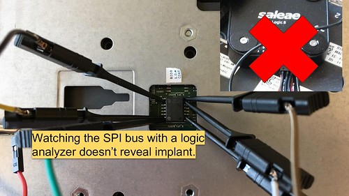 |
Attempting to detect the implant via reading the flash chips with an external programmer won't reveal the implant since it does not modify the contents of the flash chip and the read access patterns of the programmer are different from the BMC during boot, so they don't trigger it activate.
Monitoring the SPI bus during boot with a logic analyzer doesn't reveal the implant either, since the flash chip continues to output the correct data and it is modified after the series resistor. To detect the implant would require attaching the analyzer to the BGA pins on the BMC itself, which is a much more difficult task.
 Many "high assurance sites" replace their flash chips with their self-programmed versions. This doesn't necessarily work, either, since the implant data is not stored in the flash chip. This might make the implant inoperative, however, if the layout changes significantly from the version that it is expecting.
 |
 |
A sufficiently advanced hardware implant doesn't need to generate any network traffic on the BMC ethernet port, either. Since the BMC has access to either host firmware via SPI or host memory via DMA, it can inject code into the x86 and use it to exfiltrate things. One example of how this could work is the "Attacking Hypervisors via Firmware and Hardware" (PDF) (video) by Yuriy Bulygin. This attack uses SMM to allow an unprivileged guest to read all of physical memory, which could then be exfiltrated through normal guest channels without triggering any network monitoring on the BMC network.
Too many devices
 The BMC is just the start of the problem, however. As whitequark pointed out, "_PCs are just several embedded devices in a trenchcoat''", each of which has its own firmware and mutable state. Pretty much any device more complex than a resistor has firmware, and sometimes even the resistors are actually hardware implants with their own firmware.
 The NIST 800-193 Firmware Resiliency Guidelines are a good place to start for thinking about how we can treat our systems as internal networks of mutually untrusting systems and how we can reason about dealing with both detecting and recovering from compromise of different components of the system.
 Most of the 800-193 guidelines rely on devices like the Trusted Platform Module (TPM) to be able to act as a Root of Trust. I'm a big fan of TPM's for sealing data, attestation and other functions, and wish that the free software community was more interested in making use of them. They are not, however, immune to hardware implant attacks. The NCC Group's TPMGenie is able to intercept PCR extension operations and subvert the root of trust since the communication between then x86 and TPM are not authenticated.
 For that reason there is continuing innovation in different roots of trust. There are trusted execution environments like Intel SGX and ARM TrustZone, which add protected computation modes to the CPU. Many of the hyperscale companies are also developing their own hardware roots of trust as well.
The Google Titan coprocessor, which protects their servers and Chromebooks, validates the SPI flash contents prior to reset and also allows developer mode closed-case debugging for Chromebooks. Microsoft's Project Cerberus is a NIST 800-193 compliant root of trust with open firmware that allows system owners to re-key it so that they don't have to trust Microsoft as much. And Apple's T2 Security Chip has made some very significant steps in protecting the boot firmware of the Macbooks, although to the detriment of user freedom.
For that reason there is continuing innovation in different roots of trust. There are trusted execution environments like Intel SGX and ARM TrustZone, which add protected computation modes to the CPU. Many of the hyperscale companies are also developing their own hardware roots of trust as well.
The Google Titan coprocessor, which protects their servers and Chromebooks, validates the SPI flash contents prior to reset and also allows developer mode closed-case debugging for Chromebooks. Microsoft's Project Cerberus is a NIST 800-193 compliant root of trust with open firmware that allows system owners to re-key it so that they don't have to trust Microsoft as much. And Apple's T2 Security Chip has made some very significant steps in protecting the boot firmware of the Macbooks, although to the detriment of user freedom.
No More Secrets
 Contrary to Supermicro CEO's assertion that their designs are more secure because of their secrecy, I believe that openness will make our systems more secure. Servers from the Open Compute Project include full schematics, bill-of-materials, gerber files for the boards, etc. All of which motivated customers can use to validate that their hardware matches what is intended and that nothing has been added.
 Open source CPUs like RISC-V make it even more likely that we can have some trust in our systems, especially for things like the trusted execution environments. There should be no secrets in the setup and configuration of the TEE and we should be able to inspect the implementation for sidechannels or other leaks.
 |
 |
Open Hardware also requires Open Firmware to be trustable. Closed source binary blobs in our firmware makes it impossible to trust what is going on in the early stages of system initialization and also hamper efforts to detect attacks. Unless we know what is supposed to be running in the BMC or early host firmware and have a reproducible way to built it ourselves, we have no way to know what has been installed the OEM or by an attacker. The LinuxBoot project, which I co-lead with Ron Minnich of Google is a way to replace much of the proprietary host firmware with Linux and its more trusted device drivers (I gave a LinuxBoot talk at 34c3).
 We've also started the u-bmc project to apply the LinuxBoot reproducible build system to the BMC. It removes most of the legacy features that caused many of the security failures and is entirely implemented in Go, a memory safe language, which eliminates many classes of runtime security errors. Considering how much of the security of the entire systems depends on the security of the BMC, it is vital that we have better software, that we control, running there.
Conclusions
 So, did the "Big Hack" happen? ¯_(ツ)_/¯
Is it plausible? Yes, the technical details described in the article seem plausible.
What can we do about it? We need fewer secrets and better understanding of what is going on in our systems.