spispy: Open source flash emulation
 This is the very rough transcript of my presentation at CCC Camp 2019, spispy: open source flash emulation for faster firmware development and early boot security research. The 30 minute video is also available if you prefer to watch. The source
 github.com/osresearch/spispy is available if you want to jump right to hacking on it. In this presentation I want to address three questions: what are SPI flashes, why do we want to emulate them, and how do we solve the tricky real-time difficulties in doing so.
What
The first question is "what is a spi flash?". These are the small chips on a computer mainboard, frequently called "boot ROMs" although that is a bit of misnomer since they are re-writable these days and not actual ROMs. These flash chips contain the "firmware" or "BIOS" for the machine that is executed when the system is first powered on, before any of the other devices are initialized.
 The original BIOSes were proprietary to each machine
and most were fairly simple since they had to fit in
a few kilobytes of ROM chip -- they would locate
the bootloader for the operating system on a floppy
or harddisk boot block and jump into it. Most of
the BIOSes remained resident to perform basic input and output functions,
The original BIOSes were proprietary to each machine
and most were fairly simple since they had to fit in
a few kilobytes of ROM chip -- they would locate
the bootloader for the operating system on a floppy
or harddisk boot block and jump into it. Most of
the BIOSes remained resident to perform basic input and output functions,
 This firmware used to be stored in actual ROMs,
although in more modern systems it is in a non-volatile
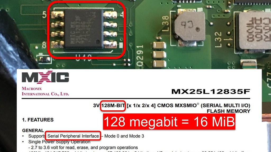
flash memory, typically in an 8 pin SOIC package.
Pulling up the datasheet for this one reveals the
expansion of the SPI acronym: Serial Peripheral Interface,
a fairly generic term for the separate clock and data
bus that it uses. Unlike the original 64 KiB BIOS chips,
modern SPI flashes are typically 64 or 128 megabits,
which is 16 or 32 MiB: not enormous, but plenty of space compared
to 64 KiB.
This firmware used to be stored in actual ROMs,
although in more modern systems it is in a non-volatile
flash memory, typically in an 8 pin SOIC package.
Pulling up the datasheet for this one reveals the
expansion of the SPI acronym: Serial Peripheral Interface,
a fairly generic term for the separate clock and data
bus that it uses. Unlike the original 64 KiB BIOS chips,
modern SPI flashes are typically 64 or 128 megabits,
which is 16 or 32 MiB: not enormous, but plenty of space compared
to 64 KiB.
 These larger chips allow significantly more complexity in the firmware,
and the proprietary Unified Extensible Firmware Interface (UEFI) firmware used by most commodity systems has
added graphics, networking and more: it's a few million lines of code and an entire operating system.
There are also open source firmware like
coreboot and linuxboot. In addition to being able to
read the source code and modify it to fit our needs, it is much simpler and reduced complexity compared
tothe closed source vendor UEFI.
These larger chips allow significantly more complexity in the firmware,
and the proprietary Unified Extensible Firmware Interface (UEFI) firmware used by most commodity systems has
added graphics, networking and more: it's a few million lines of code and an entire operating system.
There are also open source firmware like
coreboot and linuxboot. In addition to being able to
read the source code and modify it to fit our needs, it is much simpler and reduced complexity compared
tothe closed source vendor UEFI.
Why
 The second question is "why would you need to emulate the
SPI flash?".
The second question is "why would you need to emulate the
SPI flash?".
Well, if you're developing open firmware like coreboot or linuxboot, or if you are doing security research into the closed UEFI firmware, you end up having to flash new firmware images into the SPI chips over and over and over. I have spent far too much of my life waiting for these chips to flash...
Slow erase speeds
 You might think that the chips aren't very large
only 16 MiB, remember? except that they are intended to be
mostly read-only and are not optimized
for frequent writes. The chips have to be written in 4KiB
sectors, which have to be erased before they can be
re-written, and this erase time in the worst case is
120 milliseconds. So multiply 120ms by 16 MiB divide
by 4 KiB is around eight minutes for the worst case.
You might think that the chips aren't very large
only 16 MiB, remember? except that they are intended to be
mostly read-only and are not optimized
for frequent writes. The chips have to be written in 4KiB
sectors, which have to be erased before they can be
re-written, and this erase time in the worst case is
120 milliseconds. So multiply 120ms by 16 MiB divide
by 4 KiB is around eight minutes for the worst case.
 And this is every time you want to test a change
or run an experiment. So let's say that you've just
finished building coreboot and are ready to flash it.
And this is every time you want to test a change
or run an experiment. So let's say that you've just
finished building coreboot and are ready to flash it.
 |
 |
First step is that you have to power down the machine under test -- the SPI bus doesn't like having multiple devices driving it. Then you have to carefully attach your flash programmer clip to the chip.
 The you can run the flashrom or other tool to start
the write. The first few megabytes go really fast,
although that is only since the Management Engine section
hasn't changed, so no erasing is necessary..
Once it hits the BIOS region, however, it has to start erasing blocks and slows down to 30-50 KiB/s.
The you can run the flashrom or other tool to start
the write. The first few megabytes go really fast,
although that is only since the Management Engine section
hasn't changed, so no erasing is necessary..
Once it hits the BIOS region, however, it has to start erasing blocks and slows down to 30-50 KiB/s.
 |
 |
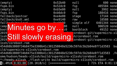
Three minutes in, still slowly erasing and rewriting at 28 KiB/s. How long is this going to take? It. Is. So. Slow.
 |
 |
Finally the flash write finishes after five and a half minutes, at a blazing average of 49 KiB/s. But it isn't time to test yet!
 |
 |
Most of the time it is necessary to remove the programmer. Maybe you can keep it attached, although the additional capacitance and loading can cause problems on the bus, so frequently you have to reattach it each time. Finally you can power the system back on and see if you forgot something stupid and have to do it all over again! SPOILER ALERT: it won't work the first ten times and you will have to keep trying different things to get coreboot to work.
Seriously I have spent so much of my time flashing these chips on so many different platforms that my flickr feed is full of these things.
The better way
 As they say in infomercials, there has to be a better way!
With spispy you attach the clip once and leave it attached to the SPI flash. Now when your coreboot or linuxboot build finishes, you can run the write command to upload the new image into the SDRAM of the spispy. Here is a video in real time flashing a new firmware with spispy
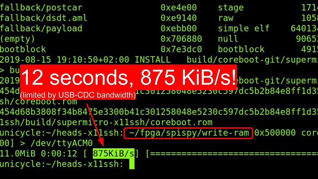 The new image is loaded in 12 seconds, with the speed
limited only by the USB-CDC-ACM bandwidth. We could
improve this since our RAM speed is hundreds of megabytes
per second, although our bottleneck will be the USB 2.0 speeds.
The new image is loaded in 12 seconds, with the speed
limited only by the USB-CDC-ACM bandwidth. We could
improve this since our RAM speed is hundreds of megabytes
per second, although our bottleneck will be the USB 2.0 speeds.
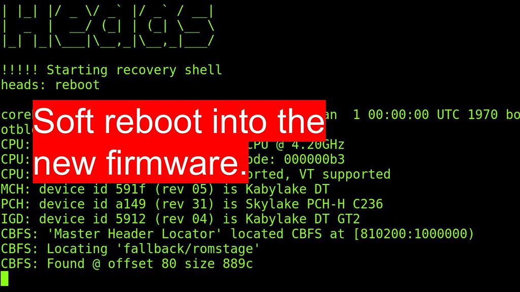 Once the new image is resident, you can soft reboot into
the new firmware without having to get out of your chair or go to the datacenter.
This greatly reduces the cycle time to test out new firmware
builds and experiment with debugging.
Once the new image is resident, you can soft reboot into
the new firmware without having to get out of your chair or go to the datacenter.
This greatly reduces the cycle time to test out new firmware
builds and experiment with debugging.
How an x86 really boots
 There's another part to the "Why" question, which is understanding what happens
in those first few milliseconds after you power on the computer.
If you've just arrived at camp from the 1970s (or even just a few years
ago), you might expect that modern x86 CPUs start the same way with a
real mode reset vector at the top of the firmware. That's no longer
the case and spispy gives us insight into is really happening during
the system startup.
There's another part to the "Why" question, which is understanding what happens
in those first few milliseconds after you power on the computer.
If you've just arrived at camp from the 1970s (or even just a few years
ago), you might expect that modern x86 CPUs start the same way with a
real mode reset vector at the top of the firmware. That's no longer
the case and spispy gives us insight into is really happening during
the system startup.
 In monitor mode it prints the addresses that are being
read from the flash so that we can analyze them.
As a quick walk through what happens
In monitor mode it prints the addresses that are being
read from the flash so that we can analyze them.
As a quick walk through what happens
- first thing we see the flash read is at offset 0x10 and 0x14, which is the Platform Controller Hub reading the Intel Flash Descriptor to verify that there is a valid flash attached.
- Then the ME starts up and reads its partition table from the flash and validates its signatures. Eventually it starts the x86.
- Which still has more to do before getting to the reset vector. Something in the x86, maybe microcode or an on-die ROM, reads the Firmware Interface Table and finds
- the microcode update entries. The correct microcode update is read and applied
- and then the bootguard authenticated code module is located and run (this platform didn't have bootguard).
- and finally, bootguard transfers control to the legacy reset vector,
- which jumps into the BIOS region. This is quite different than our time travelling visitors would have expected...
 This log of flash accesses also reveals potential security
vulnerabilities. If we plot the read address on the Y axis versus time on the X axis,
we can see that some addresses are read during a linear
scan and signature verification (called the "Time of Check"),
and then some of those same addresses are re-read again
from the flash (called "Time of Use"). If those re-reads
are not correctly validated, a malicious flash chip could
substitute new data and take control of the CPU even
with otherwise strong cryptographic signatures.
This log of flash accesses also reveals potential security
vulnerabilities. If we plot the read address on the Y axis versus time on the X axis,
we can see that some addresses are read during a linear
scan and signature verification (called the "Time of Check"),
and then some of those same addresses are re-read again
from the flash (called "Time of Use"). If those re-reads
are not correctly validated, a malicious flash chip could
substitute new data and take control of the CPU even
with otherwise strong cryptographic signatures.
 Peter Bosch and I were able to leverage this TOCTOU
attack against Intel's Bootguard and bypass their verified
boot modes. We presented the results at HITB earlier this
year in Amsterdam and this release of spispy was one of
the things we promised, so i'm very pleased to be able to go into
more details about how our system was able to emulate the SPI flash to discover this attack.
Peter Bosch and I were able to leverage this TOCTOU
attack against Intel's Bootguard and bypass their verified
boot modes. We presented the results at HITB earlier this
year in Amsterdam and this release of spispy was one of
the things we promised, so i'm very pleased to be able to go into
more details about how our system was able to emulate the SPI flash to discover this attack.
How
So that's the what and why, and since this is a very technical conference, let's get deep into the weeds of the how.
Credits
 First I want to be sure to point out that this project is
built on the wonderful work of many others. It would not
be possible to have developed it as quickly without
the excellent open source fpga toolchain of yosys,
icestorm, project trellis and nextpnr. These tools have
created an entire open source fpga ecosystem and are
a delight to use compared to the vendor tools.
First I want to be sure to point out that this project is
built on the wonderful work of many others. It would not
be possible to have developed it as quickly without
the excellent open source fpga toolchain of yosys,
icestorm, project trellis and nextpnr. These tools have
created an entire open source fpga ecosystem and are
a delight to use compared to the vendor tools.
 spispy also grew out of a collaboration with Alyssa
@noopwafel Milburn and Peter Bosch. We were hacking on things
at Revspace in Den Haag after 35c3 since Peter
and I had both noticed the potential TOCTOU and met
each other at Congress.
spispy also grew out of a collaboration with Alyssa
@noopwafel Milburn and Peter Bosch. We were hacking on things
at Revspace in Den Haag after 35c3 since Peter
and I had both noticed the potential TOCTOU and met
each other at Congress.
 We built our Bootguard POC on a small iCE40up5k FPGA,
supported by the open source icestorm tool chain.
This was sufficient for the TOCTOU that we wanted to
demonstrate -- we only needed a few kilobits of data
that easily fit in the blockram of the iCE40. The bigger problem
was deciding which TOCTOU to go after!
However, for the full spispy we realized that we needed much
more memory.
We built our Bootguard POC on a small iCE40up5k FPGA,
supported by the open source icestorm tool chain.
This was sufficient for the TOCTOU that we wanted to
demonstrate -- we only needed a few kilobits of data
that easily fit in the blockram of the iCE40. The bigger problem
was deciding which TOCTOU to go after!
However, for the full spispy we realized that we needed much
more memory.
 |
 |
And here again we benefited from the open source ecosystem. EMARD at the Croatian hackerspace Radiona had designed the ULX3S, a wonderfully full featured board around the larger and faster ecp5 FPGA supported by project trellis. It had a 32 MiB SDRAM that can read/write at around 250 MiB/s, which is plenty to keep up with the SPI bus.
 |
 |
Unfortunately SDRAM is full of dark magic with complex state transitions [that look more like alchemic transmutation diagrams. There is a large amount of complexity in interfacing with it and keeping it working reliably. Again, open source to the rescue. Stefan Kristiansson wrote https://github.com/skristiansson/wb_sdram_ctrl a verilog SDRAM controller and released it under a permissive license, allowing us to very quickly integrate the SDRAM on the ULX3S with our proof of concept SPI TOCTOU code.
 We're not the first people to try to emulate SPI flashes --
as with many projects scanlime had already done it. Her code
was dealing with smaller and slower flashes for the
Nintendo DS, although conceptionally it had many of
the same pieces that we needed to understand the bus.
We're not the first people to try to emulate SPI flashes --
as with many projects scanlime had already done it. Her code
was dealing with smaller and slower flashes for the
Nintendo DS, although conceptionally it had many of
the same pieces that we needed to understand the bus.
The SPI interface
 So let's go back to the SPI flash chips and dive back into the datasheet to better understand
what is happening on the SPI bus. As I mentioned earlier,
most of them are in an 8 pin package and we can identify
pin one from the dot on the chip. Most importantly we
can locate the power and ground on opposite corners and
be sure that we don't mix those up.
So let's go back to the SPI flash chips and dive back into the datasheet to better understand
what is happening on the SPI bus. As I mentioned earlier,
most of them are in an 8 pin package and we can identify
pin one from the dot on the chip. Most importantly we
can locate the power and ground on opposite corners and
be sure that we don't mix those up.
- The datasheet also contains timing diagrams for the signals.
- The first one to note is the Chip Select pin, which goes low when the platform controller hub is talking to the SPI flash. I've marked it here with an arrow going into the chip to indicate that it is generated from the PCH and received by the flash. We call this "negative logic" or "active low" since a 0 means selected and designate the signal with a ! or # mark in the name.
- The platform controller hub also generates the clock signal to the flash. On the falling edges of the clock the values on the data lines change and they must be stable on the rising edges. We call this "rising edge clocked", although some SPI buses are clocked on the falling edge.
- The PCH sends commands on the Serial In line to the flash. Typically there is one command byte followed by some number of argument bytes, although devices have to know how many bytes each command takes since there is no framing on the packet.
- After the command bytes, the flash responds on the Serial Out line and typically will continue to clock out bytes until the PCH raises the CS line, indicating that the transaction is over.
 The datasheet lists the command bytes and the number of
bytes that each command sends. The one that we're interested
most in emulating is the normal read, 0x03. We currently
don't support the other reads, although it would be useful
to have them implemented since they would speed up the
boot and allow us to support some other architectures.
The datasheet lists the command bytes and the number of
bytes that each command sends. The one that we're interested
most in emulating is the normal read, 0x03. We currently
don't support the other reads, although it would be useful
to have them implemented since they would speed up the
boot and allow us to support some other architectures.
 Moving to the timing diagram for the 0x03 READ, we see
that it sends the 24 address bits most significant bit
first and the flash responds with the data on the
clock immediately following the least significant
address bit.
Moving to the timing diagram for the 0x03 READ, we see
that it sends the 24 address bits most significant bit
first and the flash responds with the data on the
clock immediately following the least significant
address bit.
if (spi_done)
        spi_send( mem[spi_addr](spi_addr) )
In our blockram based proof of concept we essentially had this logic. When the last bit of address arrived, look up the contents at that address and send it on the SO line. But when we put SDRAM in there, something went wrong...
 Here the real flash is shown in blue and the emulated flash is shown in yellow.
The correct output value didn't appear on the SO line
until nearly all the way through the bit, delayed by around 50 ns.
This totally missed the timing requirements and preventing the x86 from booting.
Here the real flash is shown in blue and the emulated flash is shown in yellow.
The correct output value didn't appear on the SO line
until nearly all the way through the bit, delayed by around 50 ns.
This totally missed the timing requirements and preventing the x86 from booting.
 The reason is that SDRAM isn't "single cycle" like the
block RAM. Random reads require multiple clock cycles
to complete -- first the row and bank addresses have to
be sent, which takes a clock cycle, and then there is
a mandatory RCD (???) delay. Then the column address
is sent, another clock cycle, and the CAS latency delays
the data for another few cycles. With our 132 MHz SDRAM
clock, this is a total of 5-7 clocks and 50ns of delay.
Ironically faster memories sometimes have more latency
for a random read.
The reason is that SDRAM isn't "single cycle" like the
block RAM. Random reads require multiple clock cycles
to complete -- first the row and bank addresses have to
be sent, which takes a clock cycle, and then there is
a mandatory RCD (???) delay. Then the column address
is sent, another clock cycle, and the CAS latency delays
the data for another few cycles. With our 132 MHz SDRAM
clock, this is a total of 5-7 clocks and 50ns of delay.
Ironically faster memories sometimes have more latency
for a random read.
 Zooming in on the SPI read timing diagram, we see how
tight the requirements are, and why
that causes the problem -- with a 20 MHz SPI clock our
emulator must have the data available in roughly
half a clock, or about 25 ns. Doing a naive read from
the SDRAM won't work if it takes 50ns or more to read
a random byte from the DRAM! We need to get clever
if we're going to meet timing requirements.
Zooming in on the SPI read timing diagram, we see how
tight the requirements are, and why
that causes the problem -- with a 20 MHz SPI clock our
emulator must have the data available in roughly
half a clock, or about 25 ns. Doing a naive read from
the SDRAM won't work if it takes 50ns or more to read
a random byte from the DRAM! We need to get clever
if we're going to meet timing requirements.
 Since we're writing the fpga
logic we can be very clever indeed. We don't have to limit
ourselves to concepts like "byte boundaries" or limitations
of existing SPI hardware, nor do we need to respect the
abstraction that memory is a big array, so we can do things
like initiate the row/bank activation when the emulator has
received 14 bits of the address, overlapping tRCD with
reception of the next 9 bits, which we send to the column
address and overlap the CAS latency with receipt of the last address bit,
which we use to select the upper or lower byte of the
16-bit read result.
Since we're writing the fpga
logic we can be very clever indeed. We don't have to limit
ourselves to concepts like "byte boundaries" or limitations
of existing SPI hardware, nor do we need to respect the
abstraction that memory is a big array, so we can do things
like initiate the row/bank activation when the emulator has
received 14 bits of the address, overlapping tRCD with
reception of the next 9 bits, which we send to the column
address and overlap the CAS latency with receipt of the last address bit,
which we use to select the upper or lower byte of the
16-bit read result.
 This sort of hackery actually works! Again the real flash chip
is in blue, our emulated flash is in yellow and you
can see that our first output bit
is only a few nanoseconds slower than the real flash chip,
which is good enough to meet timing for a 20 MHz SPI bus.
We can now supply the bits to the very first read request
from the PCH with the response 0x5AA5 in msb order. Checking the hexdump of
the flash chip at the read offset 0x10 in the flash in msb oder.
This sort of hackery actually works! Again the real flash chip
is in blue, our emulated flash is in yellow and you
can see that our first output bit
is only a few nanoseconds slower than the real flash chip,
which is good enough to meet timing for a 20 MHz SPI bus.
We can now supply the bits to the very first read request
from the PCH with the response 0x5AA5 in msb order. Checking the hexdump of
the flash chip at the read offset 0x10 in the flash in msb oder.
 This is how the PCH knows that there is a valid flash
attached, as Butterworth and Kovah discuss in their
advanced x86 BIOS class. If this is not correctly read
by the PCH, the system won't start up at all.
This is how the PCH knows that there is a valid flash
attached, as Butterworth and Kovah discuss in their
advanced x86 BIOS class. If this is not correctly read
by the PCH, the system won't start up at all.
 However, while the spispy can convince the PCH to start up,
sometimes the ME fails its signature check or the Linuxboot
kernel fails its integrity checks. This is due to another
complexity of the SDRAM...
However, while the spispy can convince the PCH to start up,
sometimes the ME fails its signature check or the Linuxboot
kernel fails its integrity checks. This is due to another
complexity of the SDRAM...
 Going back to the SDRAM datasheet and that state transition
diagram...
The "auto refresh" cycle in the SDRAM controller takes over
the SDRAM every 7.8us to activate a row and "recharge"
the capacitors that are the memory cells in DRAM. While
this is happening no reads are possible for around 60ns,
which causes the flash emulator to miss its very tight
timing requirements if a refresh happens during a read.
Going back to the SDRAM datasheet and that state transition
diagram...
The "auto refresh" cycle in the SDRAM controller takes over
the SDRAM every 7.8us to activate a row and "recharge"
the capacitors that are the memory cells in DRAM. While
this is happening no reads are possible for around 60ns,
which causes the flash emulator to miss its very tight
timing requirements if a refresh happens during a read.
 Yet again, open source and flexible hardware saves us!
We can add our own refresh inhibit signal to the sdram
controller and modify the logic to prevent refresh cycles
when the SPI controller detects that a read is happening.
The 7.8us is a rough requirement, so as long as we allow
refreshes after the read transaction has completed,
then SDRAM will continue to hold data correctly.
Yet again, open source and flexible hardware saves us!
We can add our own refresh inhibit signal to the sdram
controller and modify the logic to prevent refresh cycles
when the SPI controller detects that a read is happening.
The 7.8us is a rough requirement, so as long as we allow
refreshes after the read transaction has completed,
then SDRAM will continue to hold data correctly.
 Another complication is how to prevent the real SPI flash
from responding to the read requests. You might have
noticed that most of these photos have a blue Pomona
chip clip attached and that the flash chip is still on
the mainboard - doesn't this mean that the !CS line
is going to wakeup the real flash?
Another complication is how to prevent the real SPI flash
from responding to the read requests. You might have
noticed that most of these photos have a blue Pomona
chip clip attached and that the flash chip is still on
the mainboard - doesn't this mean that the !CS line
is going to wakeup the real flash?
 It turns out that on many mainboards the !CS pin on the
SPI flash has a small series resistor between it and
the PCH's !CS output. This means that we can create
sort of an OR gate by driving the !CS line from the FPGA
and overpowering the PCH without risk of damaging either.
It turns out that on many mainboards the !CS pin on the
SPI flash has a small series resistor between it and
the PCH's !CS output. This means that we can create
sort of an OR gate by driving the !CS line from the FPGA
and overpowering the PCH without risk of damaging either.
 Schematically it looks something like this. The PCH
drives !CS low, which wakes up the real SPI flash chip
and the spispy FPGA. The SPI flash starts to drive the SO
line to send data back to the PCH, but if this is a request
that the spispy wants to handle, the fpga drives its
!CS gpio pin high. This puts the SPI flash back to sleep
and allows the fpga to take over the SO line.
Schematically it looks something like this. The PCH
drives !CS low, which wakes up the real SPI flash chip
and the spispy FPGA. The SPI flash starts to drive the SO
line to send data back to the PCH, but if this is a request
that the spispy wants to handle, the fpga drives its
!CS gpio pin high. This puts the SPI flash back to sleep
and allows the fpga to take over the SO line.
A complication is that the fpga now doesn't know when the PCH has finished the transaction, so we've added some logic that watches the CLK line for transitions. A few microseconds after no clock transitions, then FPGA assumes the transaction is over and tri-states the !CS gpio. This allows the PCH to re-assert !CS by driving it low later to start another transaction.
Status
 Putting all of these hacks together works! We can boot the
entire x86, including the PCH and ME, from the spispy and
they interact with it as if it were the real flash.
Putting all of these hacks together works! We can boot the
entire x86, including the PCH and ME, from the spispy and
they interact with it as if it were the real flash.
We've tested it on numerous laptops, desktops and a few servers. There are some academic groups who have been using it to look into early-boot security and I'm using it to assist in bringup on the first modern x86 server to support coreboot (in conjuction with 9elements and mullvad vpn).
 There are other SPI flashes that are of interest, such as the ARM based
BMC on that same server. Unfortunately we don't support some of the
commands that it uses, yet, but hopefully will be able to improve the
speed of development for openbmc or u-bmc through fixing those feature.
There are other SPI flashes that are of interest, such as the ARM based
BMC on that same server. Unfortunately we don't support some of the
commands that it uses, yet, but hopefully will be able to improve the
speed of development for openbmc or u-bmc through fixing those feature.
Help wanted
 And spispy is open source! So if you want to dive in and
help out, there are lots of areas that we would appreciate
help. One area that would make it even faster is if we
move away from USB serial and implement USB ethernet or
a custom endpoint. There are other buses in the system
that are interesting to TOCTOU, so security researchers
have at it!
And spispy is open source! So if you want to dive in and
help out, there are lots of areas that we would appreciate
help. One area that would make it even faster is if we
move away from USB serial and implement USB ethernet or
a custom endpoint. There are other buses in the system
that are interesting to TOCTOU, so security researchers
have at it!
 You can checkout the source code and tools in our github tree,
 github.com/osresearch/spispy, chat
with us on the open source firmware slack, or meet me here at camp (I'm
hanging out at the hardware hacking area). So hopefully I've answered
the what, why and how and I'd love to answer any additonal question that
you might have!