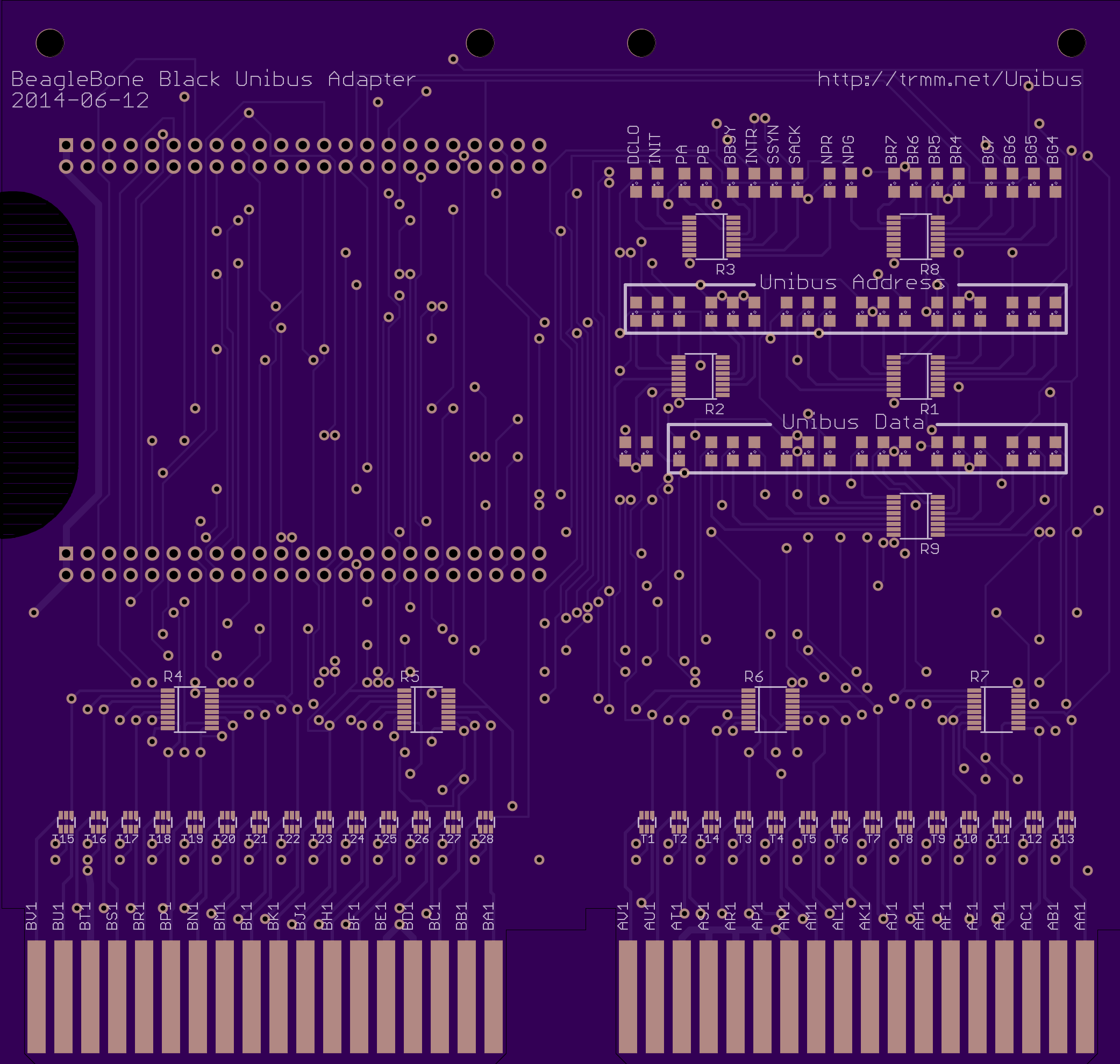
Unibus to BeagleBone Black Adapter
Unibus Adapter
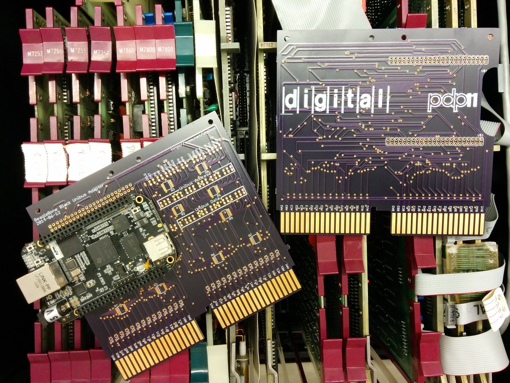 I'm building an adapter from the BeagleBone Black to the DEC Unibus to allow modern CPUs to interface with Unibus devices, or to emulate other devices on the bus, like a network adapter for our PDP-11. There are 56 signals on the bus and the BBB has 55 user GPIO lines, but the DCLO line isn't really necessary since by the time it is asserted it is too late to do anything about it.
 |
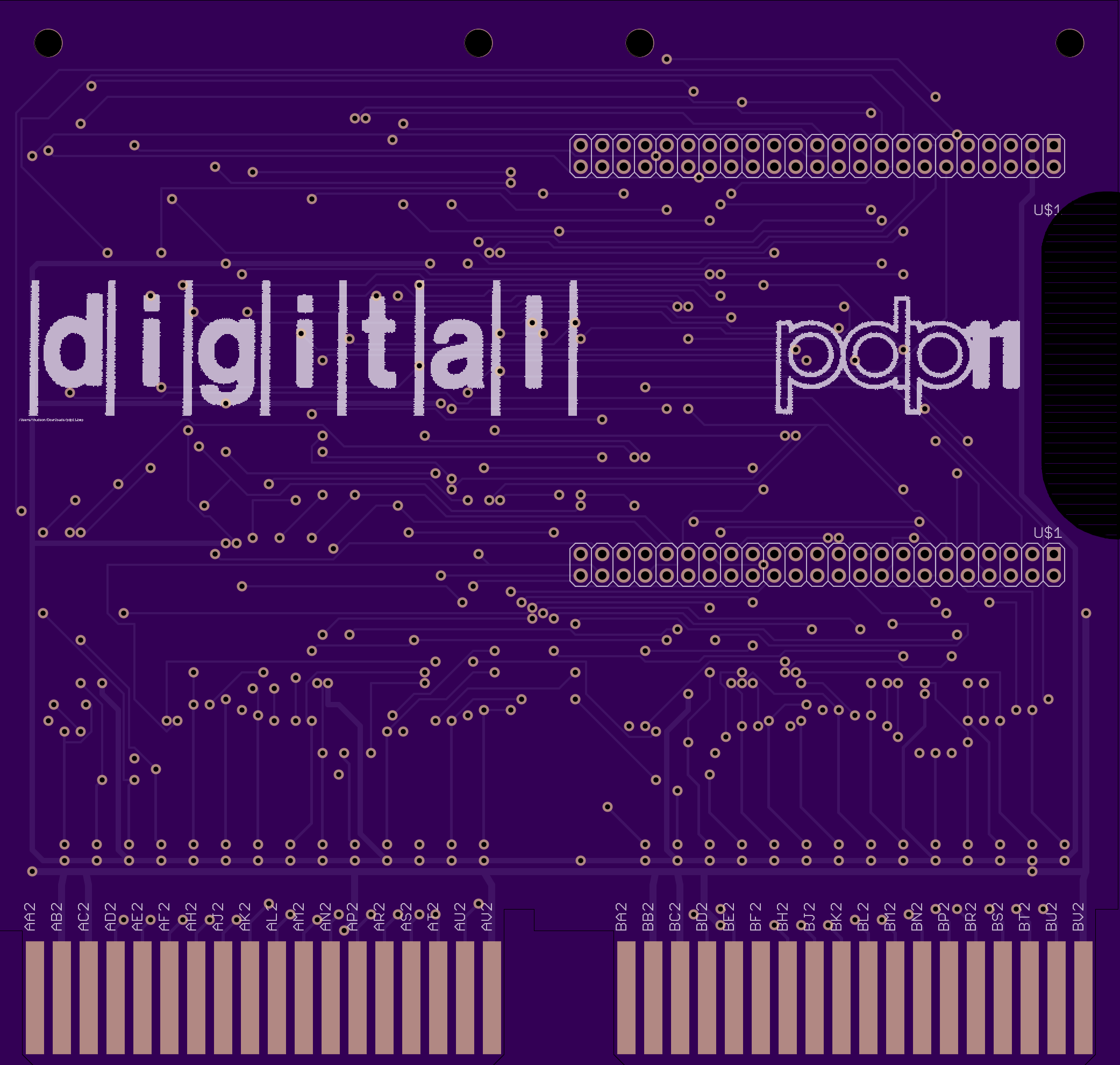 |
Board, schematic and OSH Park link, although they are untested yet. They also have a wrong package for the resistor array and a bad pinout for the MOSFET level shifters, so don't order them!
PCB details
 The 3.3V BeagleBone is interfaced to the 5V open-collector bus using the technique described in NXP appnote 10441. Due to a mistake in the board layout, the pullup resistor array is the wrong package, but this can be worked around by using the ARM's pullups. Additionally, the MOSFET package has the two drain pins swapped, so the input to the BeagleBone's GPIO is scrambled. This can be fixed by software, but means that the LEDs aren't meaningful.
Unibus pinouts

Unibus comprises ... a flat flexible cable containing 56 signal lines and 64 corresponding ground lines. The 56 signal lines are grouped logically into three types.
Initialization (3 lines): Signals on these lines control power-up, power-down, or initialization sequences of the bus devices;
Data (38 lines): These lines are used for data transfer between devices; and
Priority Arbitration (15 lines): Signals on these lines decide which device will next be allowed to control the data section.
Unibus Sections and Signal Lines Asser- No. of lion Name Mnemonic Lines Function Level Data Transfer Section Selects slave device Low Address A <17:00> 18 and/or memory address Information transfer Low Data <015:00> 16 2 Type of data transfer Control Low CO,C1 MSYN Master Sync 1 Timing control for Low data transfer Low Slave Sync SSYN 1 Parity PA, PB 2 Device parity error Low Interrupt INTR Interrupt 1 Low } Priority Arbitration Section BR4, BR5, Bus Request BR6, BR7* BG4, BG5, Bus Grant BG6, BG7* Non-Processor NPR Request Non-Processor NPG Grant SACK Selection Acknowledge BBSY Bus Busy I nitialize Section Initialize INIT AC LO AC Low DC Low DCLO 4 4 1 1 1 Requests use of bus (usually for interrupt) Grants use of bus (usually for interrupt) Requests use of bus for data transfer Grants use of bus for data transfers Acknowledges grant Low High Low High Low 1 Indicates that the data Low section is in use 1 System reset Low 1 Low 1 Low } Power monitoring
-
"BRn" and "BGn" are abbreviations used to designate that one pair of Bus Request (BR) and Bus Grant (BG) lines is used.
-
Eagle CAD files for DEC parts: http://so-much-stuff.com/pdp8/cad/cad.php
-
http://retrocmp.com/attachments/article/198/unibus_signals.txt
Unibus signals on A/B slot
from "d:\RetroCmp\dec\pdp11\unibus\pdp-11 UNIBUS DESIGN DESCRIPTION 1979.pdf"

Data Transfer, Priority Arbitration and Initialization Signals Lines

--------------------------------------------------------------------------------
                    MNEMONIC        NO.     FUNCTION
NAME            LINES           OF      LEVEL                   ASSERTION
--------------------------------------------------------------------------------
A. DATA TRANSFER SECTION

Address         A <17:00>       18      Selects slave device    Low
                                            and/or memory address
Data            D <15:00>       16      Information transfer    Low

Control*        C0, C1          2       Type of data transfer   Low

Master Sync     MSYN            1       { Timing control for    Low
Slave Sync      SSYN            1       { data transfer         Low

Parity**        PA, PB          2       Device parity error     Low

Interrupt       INTR            1       Interrupt               Low

B. PRIORITY ARBITRATION SECTION

Bus Request     BR4,BR5,BR6,BR7 4       Request use of bus      Low
                                            (usually for interrupt)

Bus Grant       BG4,BG5,BG6,BG7 4       Grant use of Bus        High
                                            (usually for interrupt)

Non-Processor   NPR             1       Request use of bus      Low
Request                                 for data transfers

Non-Processor   NPG             1       Grant use of bus        High
Grant                                   for data transfers

Selection       SACK            1       Acknowledges grant      Low
Acknowledge

Bus Busy        BBSY            1       Indicates that the      Low
                                            data section is in use

C. INITIALIZATION SECTION

Initialize      INIT            1       System reset            Low

AC Low          ACLO            1       {                       Low
                                            { Power monitoring
DC Low          DCLO            1       {                       Low


*Control lines C0, C1:
NAME         MNEMONIC    C1,C0  FUNCTION
Data In         DATI      0,0   One word of data from slave to master
Data In, Pause  DATIP     0,1   Same as DATI, but inhibits restore cycle in
                                    destructive read-out devices. Must be followed
                                    by DATO or DATOB to the same location.
Data Out        DATO      1,0   One word of data from master to slave.
Data Out, Byte  DATOB     1,1   One byte of data from master to slave.
                                    Data on D<15:08> for A00=1, D<07:00> for A00=0

**Parity Indicator PA,PB
     PA,PB
      0,0   no error in a slave in DATI/P
      0,1   error in slave in DATI/P
      1,X   reserved

LEDs are useful on:
+5V             1
INIT, ACLO, DCLO   3

*P, *G   ?   2*(4+1) = 10
SACK?           1
BBSY?           1


#########################################

Pin identifer= <Slot><Contact><Side>

                       /                                               /
                      /  1    2x20 Berg B        1     2x20 Berg A    /
                     /    :::::::::::::::         ::::::::::::::::   /
                    /                   40                       40 /
                   /              Components =                     /
                  /               Side 1                          /
                 /                                               / Solder =
                /     Slot =                       Slot =       /    Side 2
               /       B                ,_          A          /
              /                    ,___/ /                    /
             /_//////////////////_/     /_//////////////////_/
Contact = VUTSRPNMLKJHFEDCBA         VUTSRPNMLKJHFEDCBA


Signals by Backplane pin
-------------------------
            2x20                                    2x20
PIN     BERG    SIGNAL              PIN         BERG    SIGNAL

AA1     A36     INITL               BA1         B36     BG6H
AA2     A35     POWER (+5V)         BA2         B35     POWER (+5V)
AB1     A34     INTRL               BB1         B34     BG5H
AB2     A33     GROUND              BB2         B33     GROUND
AC1     A32     D00L                BC1         B32     BR5L
AC2     A31     GROUND              BC2         B31     GROUND
AD1     A30     D02L                BD1         B30     GROUND
AD2     A29     D01L                BD2         B29     BR4L
AE1     A28     D04L                BE1         B28     GROUND
AE2     A27     D03L                BE2         B27     BG4H
AF1     A26     D06L                BF1         B26     ACLOL
AF2     A25     D05L                BF2         B25     DCLOL
AH1     A24     D08L                BH1         B24     A01L
AH2     A23     D07L                BH2         B23     A00L
AJ1     A22     D10L                BJ1         B22     A03L
AJ2     A21     D09L                BJ2         B21     A02L
AK1     A20     D12L                BK1         B20     A05L
AK2     A19     D11L                BK2         B19     A04L
AL1     A18     D14L                BL1         B18     A07L
AL2     A17     D13L                BL2         B17     A06L
AM1     A16     PAL                 BM1         B16     A09L
AM2     A15     D15L                BM2         B15     A08L
AN1     A14     GROUND              BN1         B14     A11L
AN2     A13     PBL                 BN2         B13     A10L
AP1     A12     GROUND              BP1         B12     A13L
AP2     A11     BBSYL               BP2         B11     A12L
AR1     A10     GROUND              BR1         B10     A15L
AR2     A09     SACKL               BR2         B09     A14L
AS1     A08     GROUND              BS1         B08     A17L
AS2     A07     NPRL                BS2         B07     A16L
AT1     A06     GROUND              BT1         B06     GROUND
AT2     A05     BR7L                BT2         B05     C1L
AU1     A04     NPGH                BU1         B04     SSYNL
AU2     A03     BR6L                BU2         B03     C0L
AV1     A02     BG7H                BV1         B02     MSYNL
AV2     A01     GROUND              BV2         B01     GROUND


Signals by name

                    2x20                          2x20                           2x20
Signal    PIN   BERG          Signal    PIN   BERG         Signal      PIN   BERG
A00L      BH2   B23           D00L      AC1   A32          GROUND      AB2   A33
A01L      BH1   B24           D01L      AD2   A29          GROUND      AC2   A31
A02L      BJ2   B21           D02L      AD1   A30          GROUND      AN1   A14
A03L      BJ1   B22           D03L      AE2   A27          GROUND      AP1   A12
A04L      BK2   B19           D04L      AE1   A28          GROUND      AR1   A10
A05L      BK1   B20           D05L      AF2   A25          GROUND      AS1   A08
A06L      BL2   B17           D06L      AF1   A26          GROUND      AT1   A06
A07L      BL1   B18           D07L      AH2   A23          GROUND      AV2   A01
A08L      BM2   B15           D08L      AH1   A24          GROUND      BB2   B33
A09L      BM1   B16           D09L      AJ2   A21          GROUND      BC2   B31
A10L      BN2   B13           D10L      AJ1   A22          GROUND      BD1   B30
A11L      BN1   B14           D11L      AK2   A19          GROUND      BE1   B28
A12L      BP2   B11           D12L      AK1   A20          GROUND      BT1   B06
A13L      BP1   B12           D13L      AL2   A17          GROUND      BV2   B01
A14L      BR2   B09           D14L      AL1   A18          INITL       AA1   A36
A15L      BR1   B10           D15L      AM2   A15          INTRL       AB1   A24
A16L      BS2   B07           DCLOL     BF2   B25          MSYNL       BV1   B02
A17L      BS1   B08                                        NPGH        AU1   A04
ACLOL     BF1   B26                                        NPRL        AS2   A07
BBSYL     AP2   A11                                        PAL         AM1   A16
BG4H      BE2   B27                                        PBL         AN2   A13
BG5H      BB1   B34                                        POWER (+5V) AA2   A35
BG6H      BA1   B36                                        POWER (+5V) BA2   B35
BG7H      AV1   A02                                        SACKL       AR2   A09
BR4L      BD2   B29                                        SSYNL       BU1   B04
BR5L      BC1   B32
BR6L      AU2   A03
BR7L      AT2   A05
C0L       BU2   B03
C1L       BT2   B05
Retrocomputing 2014 BeagleBone